Research
Julian L. Pita Ruiz

Integrated Photonics
Design and demonstration of CMOS-compatible photonic integrated circuits on SOI and SiN platforms for high-density interconnects and sensing applications. Key components include low-loss waveguide bends, polarization-handling circuits, grating couplers, reflectors, mode converters, and multimode interferometers. Ongoing work focuses on freeform compact mode-division multiplexers and WDM devices; aluminum nitride thin-film integration on SiN waveguides; logic ports on SOI; and polarization-control devices on tellurite platforms.
Spatial Division Multiplexing
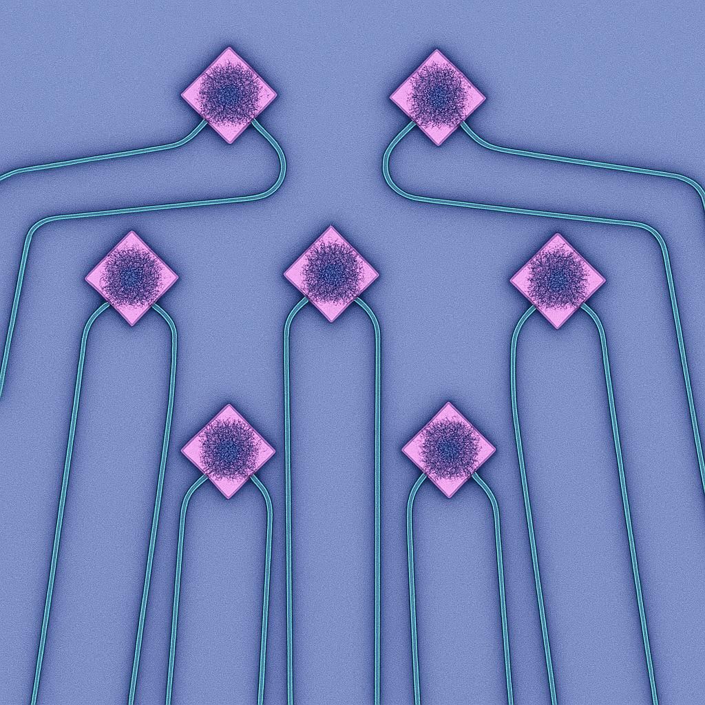
Development of ultracompact coupler interfaces for SDM fibers, including multicore and few-mode fibers, to increase data transmission capacity. Investigated optical fibers include linear 1×4 array multicore fibers, 7-core fibers, elliptical few-mode fibers, and hollow-core fibers. Research targets 100G–800G multicore fiber communication links, leveraging a seven-element freeform dual-polarization coupler array on SOI. Coupling interface development further includes a SiN multimode edge coupler capable of supporting more than 10 modes in few-mode fibers.

Inverse Design
Application of adjoint-based topology optimization to develop compact, high-performance photonic devices. Research focuses on design routines that ensure robustness against fabrication variations, particularly in low-index-contrast platforms such as silicon nitride. Emphasis is placed on translating freeform devices from simulation to fabrication by enforcing practical minimum feature sizes and incorporating prefabrication conditioning. Ongoing projects include high-visibility, high-sensitivity sensors and coupling interfaces for few-mode fibers.
Silicon Nitride Nanofabrication
Fabrication process development for SiN thin films at the INRS cleanroom, focusing on improving mechanical and optical properties for thicknesses ranging from 100 nm to ~1 µm. Research investigates crack formation in SiN films thicker than 400 nm and its evolution over time, as well as the mechanisms driving surface roughness across all thicknesses. Ongoing efforts include SiN films deposited using PECVD and LPCVD techniques and the exploration of alternative substrates such as sapphire.
Collaborators
Ongoing projects
- Inverse-designed SiN edge couplers for multimode photonics — accepted for oral presentation at OFC 2026 (collaboration with Université Laval).
- Silicon nitride arbitrary bimodal mode converter for interferometric sensors — under revision (collaboration with INRS and Aeponyx).
- Adjoint inverse design as a method for engineering photonic logic gates — under characterization (collaboration with Minas Gerais State University).
- 7×800 Gbps multicore fiber link enabled by a dual-polarization SOI coupler array — under characterization (collaboration with Corning and Ciena).
Explore microscope images, chip layouts, and experimental setups in the research gallery.